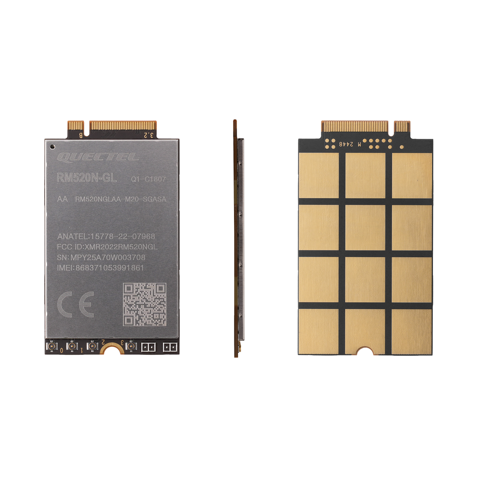
5G Module
Module Features
Core function
- Network standard: Supported 5G NR Sub-6GHz (SA/NSA)、LTE-FDD/TDD、WCDMA/HSPA+
- Interface type:M.2 Key B,supporting PCIe 3.0 x4 和 USB 3.1 Gen2
- GNSS:Integrated multi-mode positioning (GPS/GLONASS/BeiDou/Galileo/QZSS), supporting L1+L5 dual-band(AT command or hardware control)
- HPUE Enhance:Supports Class 2 power level (26 dBm), improving cell edge coverage
- Industrial-grade Design: operating temperature -40°C to +85°C, dimensions 30×52×2.3mm
Model comparison
| Type | Supported frequency bands | **HPUE frequency bands ** | GNSS |
|---|---|---|---|
| RM520N-GL | 5G: n1/n3/n5/n7/n28/n38/n40/n41/n77/n78/n79; LTE: B1/B3/B5/B7/B8/B20/B28/B38/B40/B41 | n38/n41/n77/n78/n79 | L1+L5(Reserved) |
| RM520N-EU | 5G: n1/n3/n7/n28/n41/n77/n78; LTE: B1/B3/B7/B8/B20/B28/B41 | n41/n77/n78 | L1+L5 |
| RM520N-CN | 5G: n41/n78/n79; LTE: B1/B3/B5/B8/B41 | n41/n78/n79 | L1+L5 |
Specifications
Electrical characteristic
| Parameter | Specification |
|---|---|
| Supply Voltage | 3.135V - 4.4V (Typ. 3.7V) |
| 5G Peak Power Consumption | 3.5A @ 3.7V (256QAM Modulation) |
| LTE Peak Power Consumption | 2.0A @ 3.7V (256QAM Modulation) |
| Operating Temperature | -40°C to +85°C (Industrial Grade) |
| Storage Temperature | -40°C to +90°C |
| ESD Protection | Contact Discharge ±5kV, Air Discharge ±10kV |
RF Performance
| Internet Type | Frequency Band | Downlink Rate | Uplink rate | MIMO Configuration |
|---|---|---|---|---|
| 5G NR | n41/n78(dual carrier aggregation) | 2.5 Gbps | 900 Mbps | 4×4 MIMO |
| LTE | B41(5CA) | 2 Gbps | 200 Mbps | 4×4 MIMO |
Interface Specifications
| M.2 Key B | Specifications |
|---|---|
| PCIe 3.0 | 4 channels(x4 Lane),theoretical bandwidth 32 Gbps, support NVMe protocol |
| USB 3.1 Gen2 | 10 Gbps rate, compatible with USB 2.0, support UVC protocol extension |
| (U)SIM | Dual SIM single standby, 1.8V/3.0V compatible, support hot swap (need AT+QSIMDET to enable) |
Instructions
-
Interface Configuration
- PCIe Mode Switching:
AT+QCFG="pcie/mode",1    // switch to RC mode
AT+QCFG="pcie/bandwidth",1 // configuring x4 lanes - GNSS Control:
AT+QGPS=2          // enable L1+L5 dual-frequency positioning
AT+QGPSEND        // turn off GNSS
- PCIe Mode Switching:
Precautions
Key Design Points
-
Power Supply Stability
- Transient voltage must be ≤50mV (use low ESR capacitors to suppress ripple).
- Never cut power directly. Use
AT+QPOWDcommand for soft shutdown or pullFULL_CARD_POWER_OFFlow for at least 900ms.
-
ESD Protection
- Add TVS arrays to all interfaces (junction capacitance ≤10pF).
- SIM card trace length ≤200mm with 22Ω series resistor for EMI suppression.
-
Thermal Management
- Apply thermal pads (thermal conductivity ≥5W/m·K) or heatsinks (covering module shield) during high-load operation.
- Avoid proximity to heat sources. Maintain ≥50% exposed copper area on PCB.
Safety and Maintenance
-
Prohibited Actions
- Avoid ultrasonic cleaning (damages crystals). When using alcohol to wipe, disconnect the power supply.
- In high-temperature environments (>85°C), use with derating and disable HPUE mode.
-
Firmware Upgrade
- Upgrade via USB 3.1 or PCIe interface. Ensure a stable power supply (voltage ≥3.3V).
Appendix
-
Mechanical Dimensions:330.0mm × 52.0mm × 2.3mm (M.2 Key B), ≥2.5mm clearance required for heat dissipation area.
-
Key AT Commands:
AT+CFUN=4        // Enter flight mode
AT+QSCLK=1       // Enable sleep mode
AT+QCFG="data_interface",0,0 // Switch to USB mode